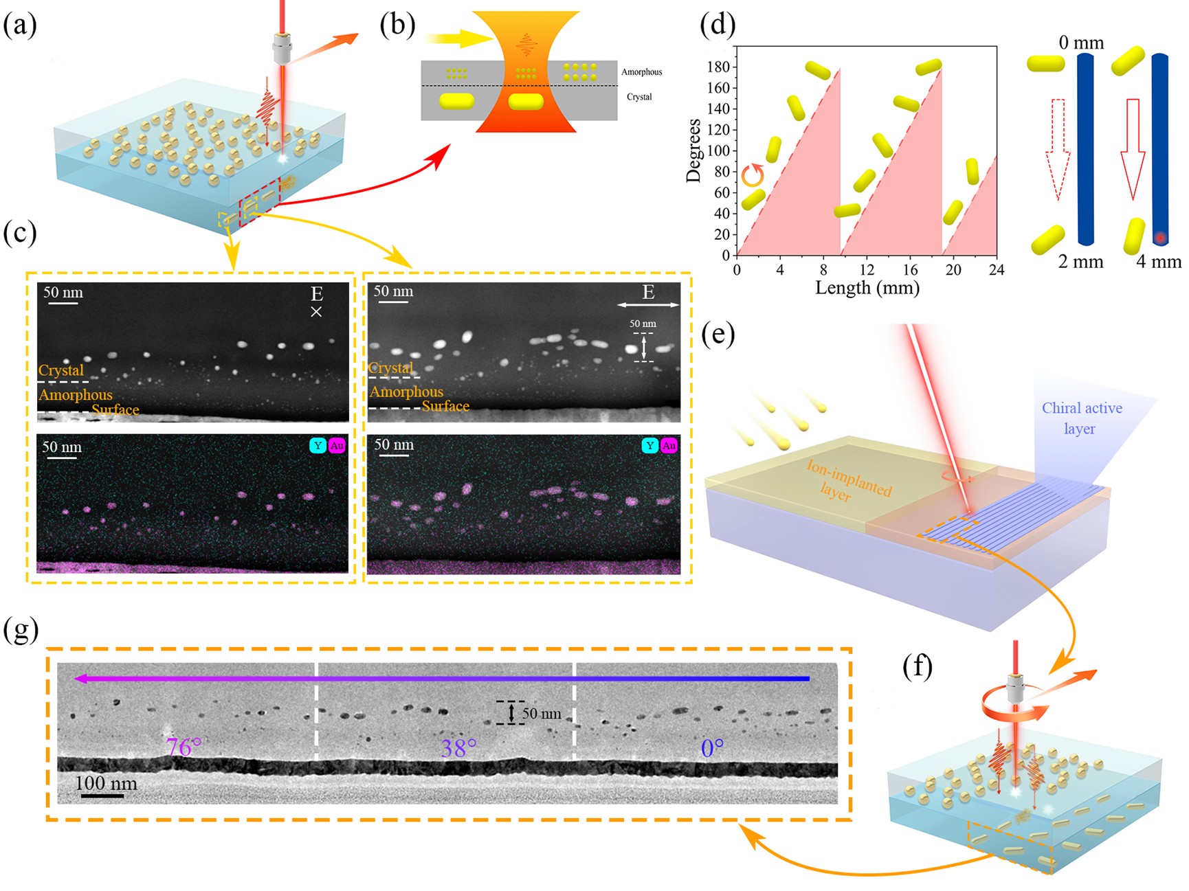
Researchers propose a novel strategy to generate optical chirality by manipulating encapsulated nanoparticles using femtosecond laser pulses
CHENGDU, SICHUAN, CHINA, October 14, 2026 /EINPresswire.com/ — Researchers propose a novel strategy to generate optical chirality by manipulating encapsulated nanoparticles using femtosecond laser pulses
Chiral materials have gained traction in photonic integrated circuits and quantum optics due to their unique capability to differentiate between spin states of light for their generation as well as detection. However, the controlled construction of large-scale chiral nanostructures in inorganic crystals remains a challenge. Now, researchers have demonstrated an innovative strategy to develop optical chirality by manipulating encapsulated nanoparticles using femtosecond laser pulses and forming rotationally arranged nanoparticles within the yttrium aluminum garnet lattice.
From the double helix of DNA to the intricate spirals of seashells, chirality is one of nature’s most elegant structural languages. An object is chiral if no combination of rotation and translation can superimpose it on its mirror image, just as a left hand cannot be made to coincide with a right hand. At its core, chirality is a form of broken symmetry. Light can carry handedness as well: the electric-field vectors of left- and right-circularly polarized light rotate in opposite directions around the propagation axis, like screws with left- or right-handed threads. Chiral optical materials that distinguish between these two forms of light provide different transmission channels for different spin states at subwavelength scales, allowing light of a particular handedness to be selectively transmitted, absorbed, or converted. This capability has made chiral materials increasingly important for encrypted optical communications, quantum-state routing, and chiral-molecule detection, while also creating new degrees of freedom in the design of on-chip integrated photonic devices.
Natural chiral materials generally exhibit limited optical responses and therefore cannot meet the diverse functional demands of practical applications. Artificial chiral materials have consequently become an important research direction, but existing routes each have shortcomings. Chemical synthesis can produce a rich variety of organic chiral materials, yet these materials often cannot withstand prolonged exposure to high temperatures, intense light, or other demanding operating conditions. Precision nanofabrication techniques, such as focused ion beam processing, can sculpt intricate structures, but they are costly and usually confine those structures to material surfaces. Inorganic optical crystals, by contrast, combine excellent mechanical strength, thermal stability, and optical performance. Encapsulating chiral structures within such crystals could yield three-dimensional optical materials that unite these advantages. Yet a crystal lattice is not a blank sheet on which arbitrary patterns can be drawn: the controlled construction of embedded chiral nanostructures inside a crystal remains a formidable challenge.
Metal nanoparticles (NPs) offer a promising way to address this challenge. When driven by a light field, the free electrons in these particles oscillate collectively, a phenomenon known as localized surface plasmon resonance that confines optical energy to nanoscale regions. This effect magnifies subtle changes in particle shape, orientation, or arrangement into measurable differences in optical response. Metal NPs buried in advance inside a crystal can therefore serve as structures that may be deliberately reconfigured after embedding. Femtosecond lasers are well suited to this task. Their pulses last on the order of one quadrillionth of a second, and their energy can be confined to an extremely small focal region. They can therefore penetrate transparent materials and finely modify internal nanostructures while leaving the surrounding lattice largely undisturbed. As the technology has advanced, femtosecond lasers have evolved from tools for simply changing material properties into instruments capable of directing the evolution of NPs inside glasses and crystals.
In this work, a joint team from Shandong University, China; Shanghai Institute of Optics and Fine Mechanics of Chinese Academy of Sciences, China; Swinburne University of Technology, Australia; and Helmholtz-Zentrum Dresden-Rossendorf, Germany, proposed a top-down two-step strategy for the controllable synthesis of chiral nanostructures inside optical crystals. The research team first encapsulated gold NPs in yttrium aluminum garnet crystals, then used a femtosecond laser with continuously varying polarization direction to manipulate them. The concentrated, ultrashort laser energy reshaped and rearranged the originally near-spherical particles into gold nanorods with varying orientations. Differences in nanorod orientation and depth broke the crystal’s original mirror symmetry, giving the material a chiroptical response capable of distinguishing left- from right-circularly polarized light. Experimental measurements and numerical simulations jointly confirmed that reversing the direction in which the laser polarization rotated produced nanostructures of opposite handedness. Adjusting the laser-processing parameters also tuned the chiroptical response across the visible to near-infrared range. The team subsequently incorporated these chiral structures into optical waveguides, causing circularly polarized light of opposite handedness to emerge with different output intensities after transmission. This result not only established that the material possessed measurable chirality but also demonstrated its potential for integration into photonic devices. The work was published online in Opto-Electronic Advances, entitled “Femtosecond laser inscribed 3D optical chirality” on September 07, 2026.
Unlike conventional precision machining of solid materials, the team’s approach uses ultrafast laser pulses to actively trigger the reorganization of nanoscale structures already inside the crystal, thereby endowing the material with tunable optical functions. One of the study’s most important features is that the chiral nanostructures are constructed in situ within an optical crystal at room temperature and atmospheric pressure. Conventional chiral nanostructures are commonly fabricated on material surfaces, where they are vulnerable to wear, contamination, and environmental changes. By contrast, the gold nanostructures in this work are enclosed in three dimensions by the crystal and closely integrated with the surrounding lattice, potentially giving them greater long-term durability. Femtosecond laser direct writing also offers high spatial selectivity, adjustable processing parameters, and flexible design. Without assembling NPs one by one, it can reshape and organize them according to predetermined requirements, opening a possible route to large-area, low-cost, and customized manufacturing. The study connects nanoscale material control with optical-device construction and demonstrates a complete path from chiral-structure design to polarization-selective light transmission. As the technology matures, it could enable more accessible nanofabrication, smaller optical components, and more highly integrated optical communication systems.
Several challenges remain before this proof of principle can become a practical device. Researchers need to strengthen the material’s ability to distinguish the two circular polarizations, reduce intrinsic propagation losses in the waveguide, and improve the uniformity and reproducibility of nanostructures across large processing areas so that the method can meet the performance requirements of specific optical applications. More precise quantitative relationships must also be established between power, scanning speed, polarization changes of laser and morphology, and optical properties of NPs. This would shift structural design from empirical adjustment toward predictable, programmable manufacturing. Future studies could extend the approach to other metal NPs and optical crystal systems, explore more complex three-dimensional arrangements and broader operating wavelength ranges, and increase fabrication throughput through parallel direct writing. As these challenges are addressed, the interior of a crystal could become an on-demand, three-dimensional optical space capable of generating, guiding, filtering, sensing, and processing light on a single material platform.
Reference
Title of original paper: Femtosecond laser inscribed 3D optical chirality
Journal: Opto-Electronic Advances
DOI: 10.29026/oea.2026.260017
About Professor Feng Chen from Shandong University, China
Dr. Feng Chen is a Professor at Shandong University, China. He is a Fellow of the Institute of Physics (IOP), SPIE, and Optica. His research focuses primarily on nanophotonic structures and devices, ion-beam modification of materials, ultrafast laser nanofabrication, single-crystal lithium niobate thin films, and topological photonics. He has published more than 400 SCI-indexed papers and delivered over 70 keynote and invited presentations at international academic conferences. He has also served as an organizer for numerous international and national conference series including CLEO, CLEO Europe, CIOP, and MRS-J.
Siyi Ma
Institute of Optics and Electronics, Chinese Academy of Scie
oej_publishing@ioe.ac.cn
+86 19136186296
Legal Disclaimer:
EIN Presswire provides this news content “as is” without warranty of any kind. We do not accept any responsibility or liability
for the accuracy, content, images, videos, licenses, completeness, legality, or reliability of the information contained in this
article. If you have any complaints or copyright issues related to this article, kindly contact the author above.

Media gallery